


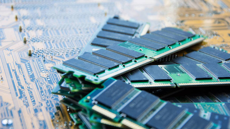


DRAM
Accelerate your time to market with quality DRAM components — rigorously tested for a wide range of applications. From the extreme temperature and performance needs of industrial and automotive applications to the exacting specs of enterprise systems, we have the right memory solution for your design.
产品详情
Accelerate your time to market with quality DRAM components — rigorously tested for a wide range of applications. From the extreme temperature and performance needs of industrial and automotive applications to the exacting specs of enterprise systems, we have the right memory solution for your design.
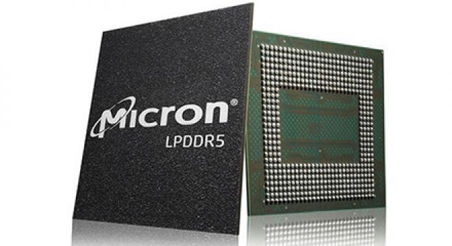
Product:DDR5 SDRAM、DDR4 SDRAM、DDR3 SDRAM、DDR2 SDRAM、DDR SDRAM、SDRAM、RLDRAM Memory、LPDRAM
| Feature/Option | DDR4 | DDR5 | DDR5 Advantage |
|---|---|---|---|
| Data rates | 1600-3200 MT/s | 3200-6400 MT/s | Increases performance and bandwidth |
| VDD/VDDQ/VPP | 1.2/1.2/2.5 | 1.1/1.1/1.8 | Lowers power |
| Internal VREF | VREFDQ | VREFDQ, VREFCA, VREFCS | Improves voltage margins, reduces BOM costs |
| Device densities | 2Gb-16Gb | 8Gb-64Gb | Enables larger monolithic devices |
| Prefetch | 8n | 16n | Keeps the internal core clock low |
| DQ receiver equalization | CTLE | DFE | Improves opening of the received DQ data eyes inside the DRAM |
| Duty cycle adjustment (DCA) | None | DQS and DQ | Improves signaling on the transmitted DQ/DQS pins |
| Internal DQS delay monitoring | None | DQS interval oscillator | Increases robustness against environmental changes |
| On-die ECC | None | 128b+8b SEC, error check and scrub | Strengthens on-chip RAS |
| CRC | Write | Read/Write | Strengthens system RAS by protecting read data |
| Bank groups (BG)/banks | 4 BG x 4 banks (x4/x8) 2 BG x 4 banks (x16) | 8 BG x 2 banks (8Gb x4/x8) 4 BG x 2 banks (8Gb x16) 8 BG x 4 banks (16-64Gb x4/x8) 4 BG x 4 banks (16-64Gb x16) | Improves bandwidth/performance |
| Command/address interface | ODT, CKE, ACT, RAS, CAS, WE, A<X:0> | CA<13:0> | Dramatically reduces the CA pin count |
| ODT | DQ, DQS, DM/DBI | DQ, DQS, DM, CA bus | Improves signal integrity, reduces BOM costs |
| Burst length | BL8 (and BL4) | BL16, BL32 (and BC8 OTF, BL32 OTF) | Allows 64B cache line fetch with only 1 DIMM subchannel. |
| MIR (“mirror” pin) | None | Yes | Improves DIMM signaling |
| Bus inversion | Data bus inversion (DBI) | Command/address inversion (CAI) | Reduces VDDQ noise on modules |
| CA training, CS training | None | CA training, CS training | Improves timing margin on CA and CS pins |
| Write leveling training modes | Yes | Improved | Compensates for unmatched DQ-DQS path |
| Read training patterns | Possible with the MPR | Dedicated MRs for serial (userdefined), clock and LFSR -generated training patterns | Makes read timing margin more robust |
| Mode registers | 7 x 17 bits | Up to 256 x 8 bits (LPDDR type read/write) | Provides room to expand |
| PRECHARGE commands | All bank and per bank | All bank, per bank, and same bank | PREsb enables precharging-specific bank in each BG |
| REFRESH commands | All bank | All bank and same bank | REFsb enables refreshing of specific bank in each BG |
| Loopback mode | None | Yes | Enables testing of the DQ and DQS signaling |